Bare blinky
I have messed with electronics for quite some time now, pretty much ever since I started programming. Actually, I learned basic C programming by playing in Arduino IDE. So I have a decent understanding of how to write basic programs that run on Arduino-like compatible microcontrollers; but I have a mediocre understanding of what is actually going on when I use the Arduino or, even, the own chip’s framework. So I want to go down the software stack and understand exactly what really happens under the hood. I think making an LED blink, an extremely basic task, in assembly and without any libraries/frameworks is a decent starting point.
Setup
I bought a CH32V003 kit a while back with this goal in mind. It’s a microcontroller based on QuingKe RISC-V2A with 2KB SRAM, 16KB FLASH, PFIC and comes with a bunch of very common peripherals (e.g. I2C, USART, SPI, ADC, etc). The kit also includes a WCH-LinkE, a USB to SWIO bridge, which is used to program the microcontroller and monitor the USART interface.
I am using PlatformIO to manage the project, although that isn’t really relevant to this post. All of the code can be found on my GitHub repository.
Plan
The CH32V003 kit’s PCB has an LED connected to GPIO D4 which emits light when that pin is low. So we need a way to manipulate the GPIO pin. Then we need a way to time the actions perfomed on the GPIO pin, so that the LED actually blinks and it does so at a constant rate.
The following block diagram depicts the CH32V003 system architecture:
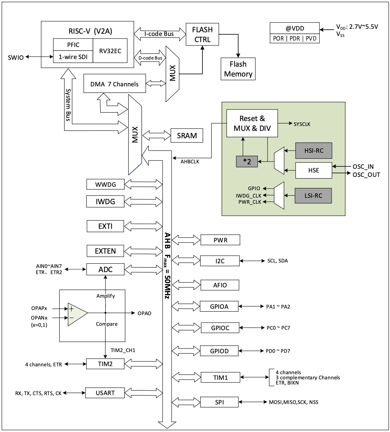
There are three GPIO ports: GPIOA (PA1-PA2), GPIOC (PC0-PC7) and GPIOD (PD0-PD7) which are completely seperate GPIO controllers. Like most peripherals, they are accessed through the AHB bus. Each of these peripheral controllers has a set of registers that control the behaviour of the actual peripheral, and each of these registers is wired to the bus. Additionally, although not specified in the block diagram, the CH32V003 core has a system tick counter which we can use to time the GPIO actions. Like the peripherals on the AHB bus, it has a set of registers that control its behaviour.
This is what’s called Memory Mapped IO, and it is very common in microcontrollers. The registers from the peripheral controllers are each assigned a unique memory address. Therefore, interfacing with each register translates to a read and/or write operation from/to the bus. The CH32V003 has the following memory map:
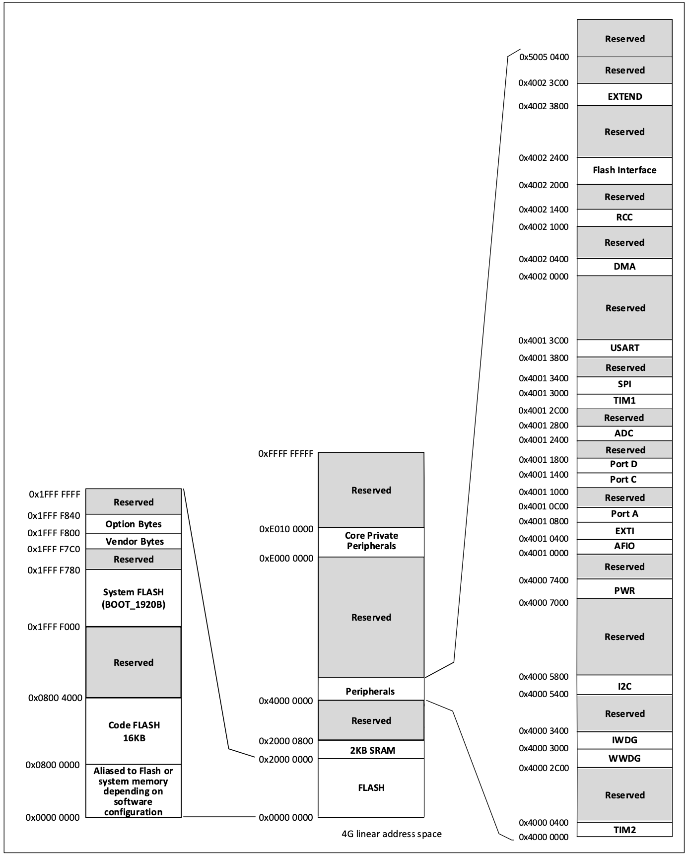
Note that FLASH and SRAM are also peripherals and, while they are connected on different buses, are accesed in the same way as any other peripheral. This means that all components are wired in a way such that when the RISC-V2A core selects an address to read/write to, the correct bus and peripheral controller register is enabled and given access to the bus. So to us, the RISC-V2A core programmers, accessing any peripheral is analogous to reading/writing data to memory.
According to the memory map diagram, the GPIO port D registers are located between addresses 0x40011400 and 0x40011800, and, though not specified, the system tick timer’s registers are located in the Core Private Peripherals section (0xe000000 to 0xe0100000).
System clock setup
Before setting anything else up we should initialize the system clock. After reset, the CH32V003 uses the HSI (High Speed Internal) oscillator at 24MHz as a clock source. The PLL (Phase Locked Loop), used to multiply the input clock source, is disabled. An HSE (High Speed Extenal) oscillator 4-25MHz can also be used as a clock source which is disabled after reset; up to de user to set it up on every startup.
The following block diagram shows the system clock tree:
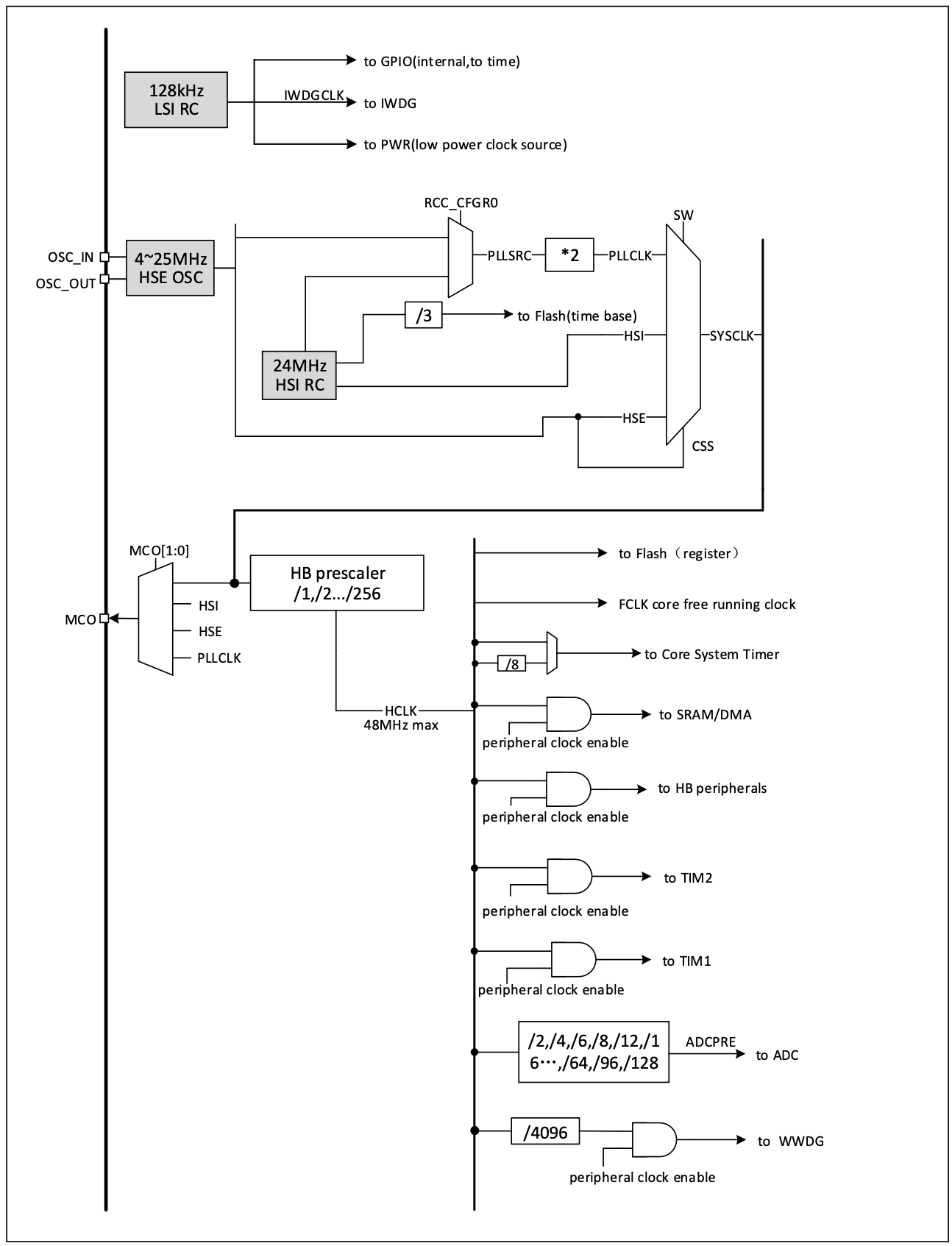
A few important notes about the clock tree that we should care about:
HSEandHSIcan multiplied by 2 through aPLL, soSYSCLKoutput is multiplexed betweenHSI,HSE,HSI*2andHSE*2HCLKis prescaled (divisible by: 1, 2, …, 256) fromSYSCLKHCLKis used for HB peripherals (GPIO)HCLKis used for Core System Timer and can be divided by 8 (useful for longer timer delays)
Because HCLK depends on SYSCLK, let’s configure SYSCLK first. We’ll configure it at 48MHz; the maximum supported frequency. Because we don’t have an external crystal (HSE), we’ll use the internal oscillator (HSI) which runs at 24MHz and feed it to the PLL to multiply it by 2 (24MHz * 2 = 48MHz). So first of all, we have to enable both HSI and PLL and configure HSI as PLL source. Then, because we’ll need to kwow when PLL is ready before we can actually select it as a clock source, we should clear RCC interrupt flags. These flags indicate the state of different clock devices and are used to detect when different events happen, and PLL being ready is one of them. Because these flags don’t auto-reset we have to reset them so that we can detect when PLL is ready. The next obvious step to finish SYSCLK configuration would be to select HSI+PLL (HSI*2) by selecting PLL as clock source, but before we do that we should configure everything that depends on SYSCLK so that when we do enable it everything else is setup and ready to go. For our use case there are two things to configure: HCLK prescaler configuration (we want to turn it off so that HCLK = SYSCLK = 48MHz) and flash with a 1 cycle latency (this is recommended in the reference manual when 24MHz <= SYSCLK <= 48MHz). The last thing to do is to wait for the PLL to be ready, select it as SYSCLK source and wait until it is actually used as SYSCLK before executing the rest of the program.
Because some of the steps detailed above can be perfomed at the same time we can optimise the list of steps to look like this:
- Enable HSI and PLL
- Select HSI as PLL source and turn off prescaler
- Clear RCC interrupt flags
- Configure flash to use 1 cycle latency
- Wait until PLL is ready
- Select PLL as SYSCLK
- Wait until PLL is used as SYSCLK
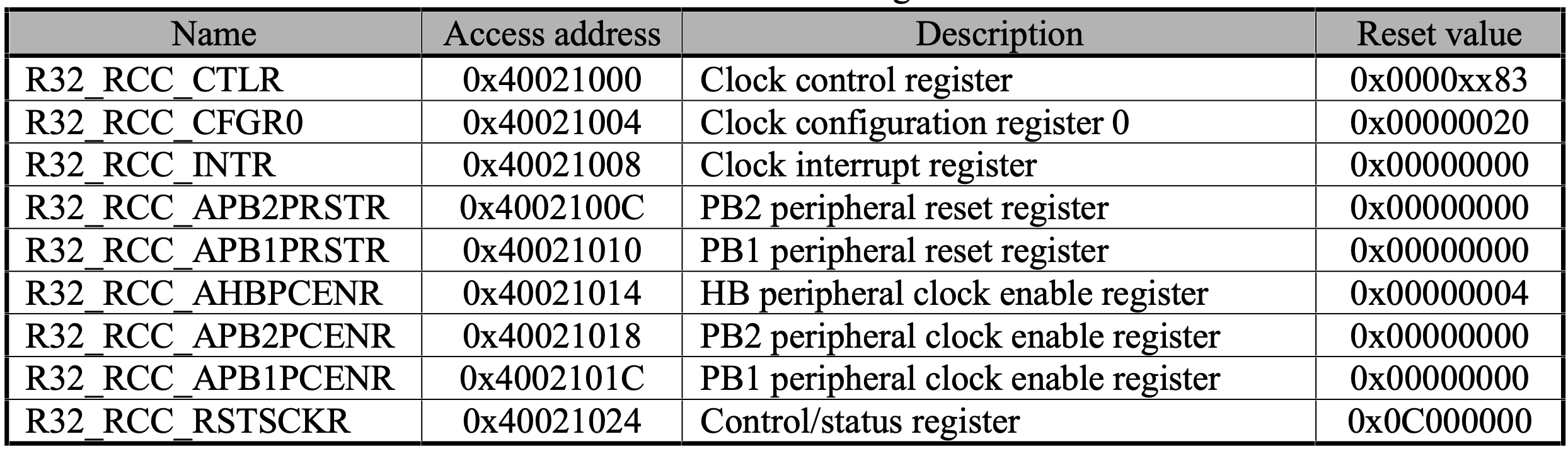
All of these steps are performed using the RCC (Reset and Clock Control) registers, with base address 0x40021000:
and the FLASH registers, with base address 0x40022000:
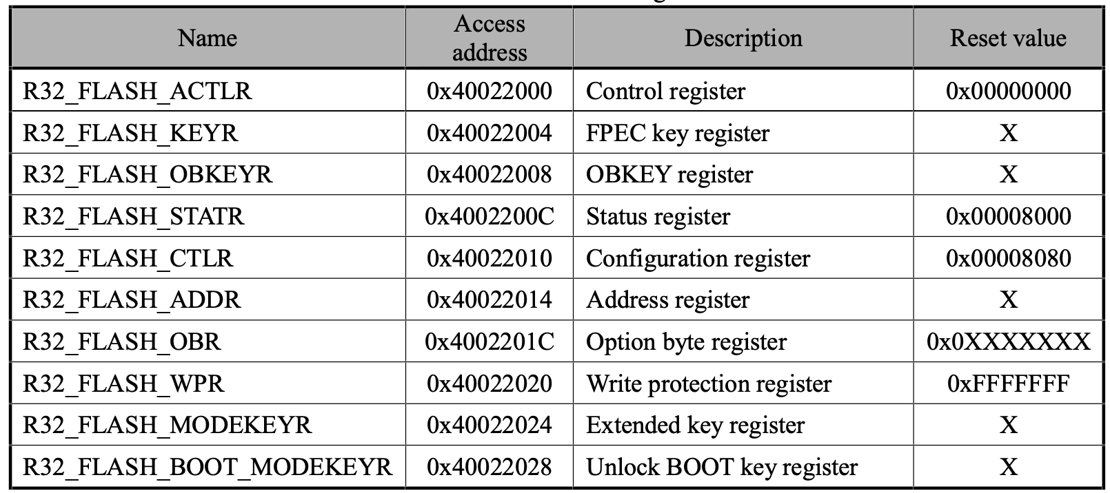
More specifically, we’ll need the following registers:
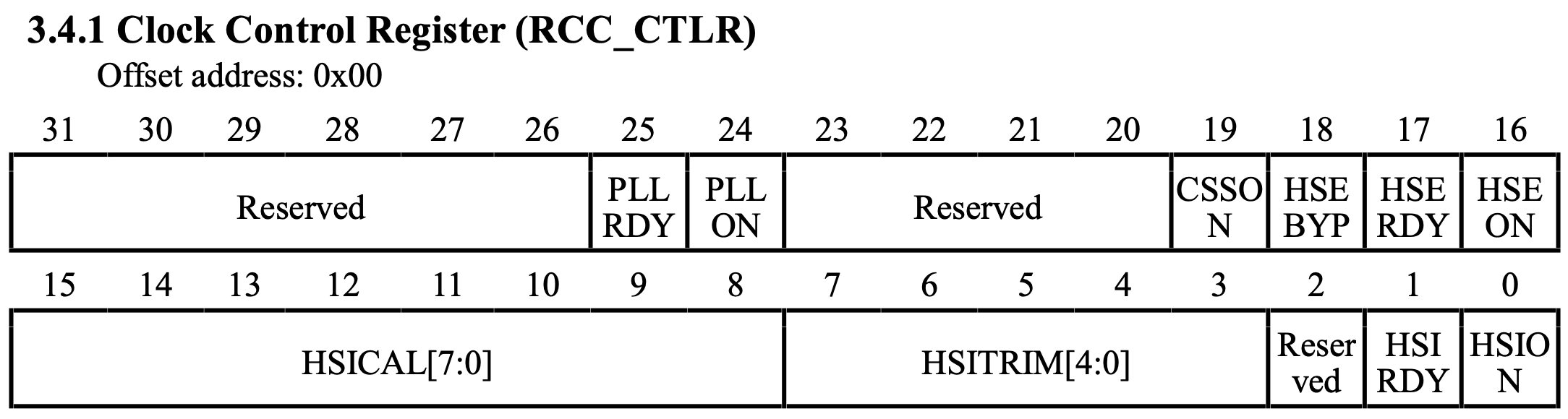
R32_RCC_CTLR
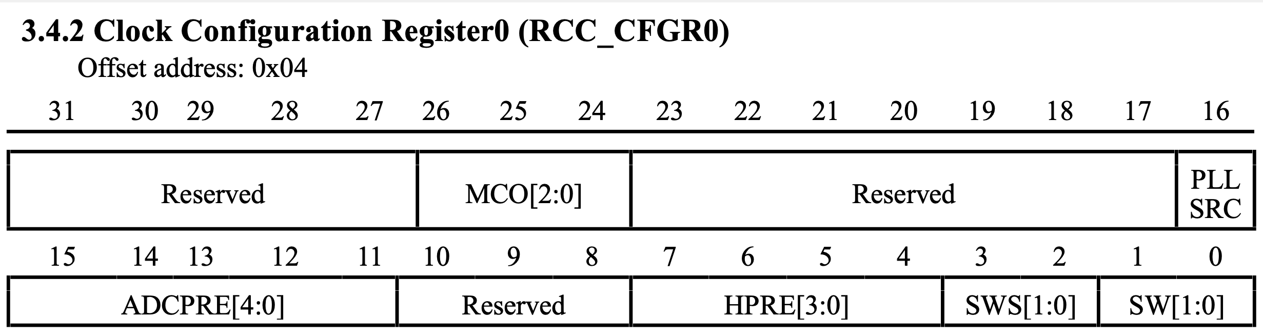
R32_RCC_CFGR0
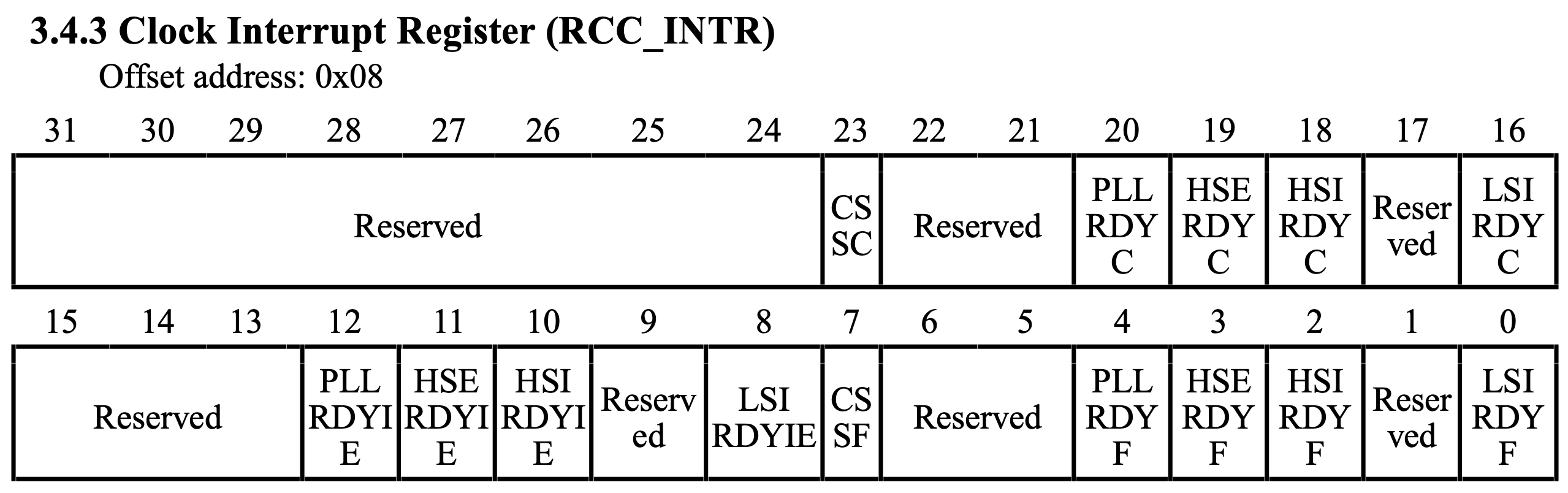
R32_RCC_INTR
R32_FLASH_ACTLR
Note: the description of each field for all registers is left out for brevity. More information can be found in the reference manual.
Enable HSI and PLL
HSI and PLL are enabled through R32_RCC_CTLR field HSION (bit 0) and field PLLON (bit 24). For both fields, writing a 1 will enable the device and writing a 0 will disable it. So let’s write some RISC-V assembly code that enables them both:
.equ rcc_base, 0x40021000
.equ flash_r_base, 0x40022000
.equ gpio_pd_base, 0x40011400
.equ systck_base, 0xe000f000

.equ led_pin, 4

.globl main
main:
        li a0, rcc_base # a0 -> RCC register base address
        li a1, flash_r_base # a1 -> FLASH register base address
        li a2, gpio_pd_base # a2 -> GPIO port d register base address

        # PLL_ON (bit 0): enable PLL
        # HSI_ON (bit 24): enable HSI
        #     RCC CTLR = 1 << 0 | 1 << 24
        #     RCC CTLR = 0x01000001
        li t0, 0x01000001
        sw t0, 0(a0)
Note: a few lines of code have been added, like constant definitions, which will be needed later.
Select HSI as PLL source and turn off prescaler
The prescaler is turned off by writing 0 to R32_RCC_CFGR0 field HPRE (bits 4-7) and HSI is selected as PLL source by writing 0 to field PLLSRC (bit 16):
        # HPRE = 0: prescaler off; do not divide SYSCLK
        # PLLSRC = 0: HSI (instead of HSE) for PLL input
        #     RCC_CFGR0 = 0 << 4 | 0 << 16
        #     RCC_CFGR0 = 0
        li t0, 0x00000000
        sw t0, 4(a0)
Clear RCC interrupt flags
Clearing the RCC interrupt flags, actually involves all R32_RCC_INTR fields, so let’s take a closer look at them to better understand how this register works:
| bit | name | access | description |
|---|---|---|---|
| 0 | LSIRDYF | RO | LSI clock-ready interrupt flag |
| 2 | HSIRDYF | RO | HSI clock-ready interrupt flag |
| 3 | HSERDYF | RO | HSE clock-ready interrupt flag |
| 4 | PLLRDYF | RO | PLL clock-ready lockout interrupt flag |
| 7 | CSSF | RO | Clock security system interrupt flag bit |
| 8 | LSIRDYIE | RW | LSI ready interrupt enable bit |
| 10 | HSIRDYIE | RW | HSI ready interrupt enable bit |
| 11 | HSERDYIE | RW | HSE ready interrupt enable bit |
| 12 | PLLRDYIE | RW | PLL ready interrupt enable bit |
| 16 | LSIRDYC | WO | Clear the LSI oscillator ready interrupt flag bit |
| 19 | HSERDYC | WO | Clear the HSE oscillator ready interrupt flag bit |
| 18 | HSIRDYC | WO | Clear the HSI oscillator ready interrupt flag bit |
| 20 | PLLRDYC | WO | Clear the PLL ready interrupt flag bit |
| 23 | CSSC | WO | Clear the clock security system interrupt flag bit |
The first 5 table entries are interrupt flags, indicated by the trailing F, and are read-only because they are set by hardware. The last 5 table entries are fields used to clear the interrupt flags, indicated by the trailing C, and are write-only. Because the interrupt flags are set by hardware, these fields are needed to physically “reset” the corresponding hardware, which will in turn clear the corresponding interrupt flag. Finally, the middle 4 table entries are interrupt enable fields, indicated by the trailing IE. When set to 1 an interrupt will be generated when the corresponding interrupt flag is set.
For our use case, we actually only need to clear certain interrupt flags in order to know when certain events happend (e.g. we’ll need to know when PLL is ready after we have enabled it), but clearing all of the interrupt flags is a good idea when changing the clock tree configuration anyway, so we’ll do that. Also, we could write our program in a way that doesn’t actively wait for the peripherals to be ready by utilizing interrupts but that would complicate our code, so we’ll disable interrupts too:
        # CSSC     (bit 23) = 1 -> clear CSSF (clock security system interrupt flag bit)
        # PLLRDYC  (bit 20) = 1 -> clear PLLRDYF (PLL-ready interrupt flag bit)
        # HSERDYC  (bit 19) = 1 -> clear HSERDYF (HSE oscillator ready interrupt flag bit)
        # HSIRDYC  (bit 18) = 1 -> clear HSIRDYF (HSI oscillator ready interrupt flag bit)
        # LSIRDYC  (bit 16) = 1 -> clear LSIRDYF (LSI oscillator ready interrupt flag bit)
        # PLLRDYIE (bit 12) = 0 -> disable PLL-ready interrupt
        # HSERDYIE (bit 11) = 0 -> disable HSE-ready interrupt
        # HSIRDYIE (bit 10) = 0 -> disable HSI-ready interrupt
        # LSIRDYIE (bit  8) = 0 -> disable LSI-ready interrupt
        #     RCC_INTR = 1<<23 | 1<<20 | 1<<19 | 1<<18 | 1<<16 | 0<<12 | 0<<11 | 0<<10 | 0<<8
        #     RCC_INTR = 0b 0000 0000 1001 1101 0000 0000 0000 0000
        #     RCC_INTR = 0x009d0000
        li t0, 0x009d0000
        sw t0, 8(a0)
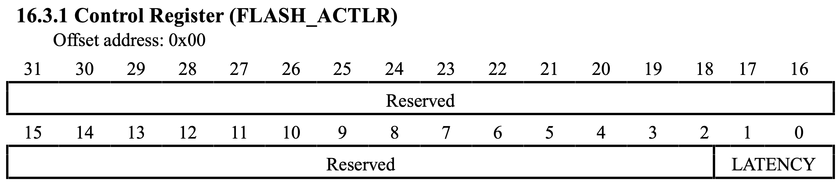
Configure flash to use 1 cycle latency
Flash latency is configured through R32_FLASH_ACTLR field LATENCY (bits 0-1); writing a 1 will select a 1 cycle latency:
        # configure flash to recommended settings for 48MHz clock
        # LATENCY (bits 0-1) = 1
        #     FLASH_ACTLR = 1 << 0
        #     FLASH_ACTLR = 1
        li t0, 0x00000001
        sw t0, 0(a1)
Wait until PLL is ready
When PLL is ready RCC_CTLR field PLLRDY (bit 25) will be set to 1. So we could write a loop that iterates until PLLRDY is set:
        # wait until PLL is ready
        li t1, 0x02000000 # PLL_RDY mask = 1 << 25
.L_pll_rdy_wait:
        lw t0, 0(a0)
        and t0, t0, t1
        beq t0, zero, .L_pll_rdy_wait
Select PLL as SYSCLK
Once PLL is ready we can select it as SYSCLK source, which is done by setting R32_RCC_CFGR0 field SW (bits 0-1) to 2. Because we don’t want to modify the rest of the fields we could read the register value, set the first two bits to 0 with a bitwise AND mask (which would be 0b11 << 0 = 0x00000003) and then bitwise OR the result with 2:
        # RCC_CFGR0 = RCC_CFGR0 & ~(0b11) | 0b10
        # RCC_CFGR0 = RCC_CFGR0 & ~(0x00000003) | 0x00000002
        # RCC_CFGR0 = RCC_CFGR0 & 0xfffffffc | 0x00000002
        lw t0, 4(a0) # t0 = RCC_CFGR0
        and t0, t0, 0xfffffffc # clear clock source selection ~(0x00000003) = 0xfffffffc
        or t0, t0, 0x00000002 # select PLL as clock source 0x00000002
        sw t0, 4(a0)
Wait until PLL is used as SYSCLK
When PLL is selected as clock source R32_RCC_CFGR0 field SWS (bits 2-3) will be set to 2 (the same value we set field SW to in the previous step). We could write a loop that iterates until SWS is set to 2:
        # wait until PLL is used as SYSCLK
        li t1, 0x0000000c # RCC_CFGR0 SWS mask
        li t2, 0x00000008 # RCC_CFGR0 SW PLL
.L_pll_use_wait:
        lw t0, 4(a0)
        and t0, t0, t1
        bne t0, t2, .L_pll_use_wait
GPIO port setup
Before we can set a pin high or low we have to enable the corresponding GPIO port and configure the individual pin as output.
Enabling the GPIO port is done through R32_RCC_APB2PCENR field IOPDEN (bit 5) which enables (when set to 1) disables (when set to 0) GPIO port D clock:
        # setup GPIO pin for led
        # enable GPIO port D clock
        # RCC_AP2PCENR = RCC_AP2PCENR | 1 << 5
        # RCC_AP2PCENR = RCC_AP2PCENR | 0x00000020
        lw t0, 24(a0) # t0 = APB2PCENR
        or t0, t0, 0x00000020 # APB2PCENR | EPB2PCENR_IOPDEN
        sw t0, 24(a0)
Configuring the GPIO pin involves the GPIO registers, where each port has a different base address:
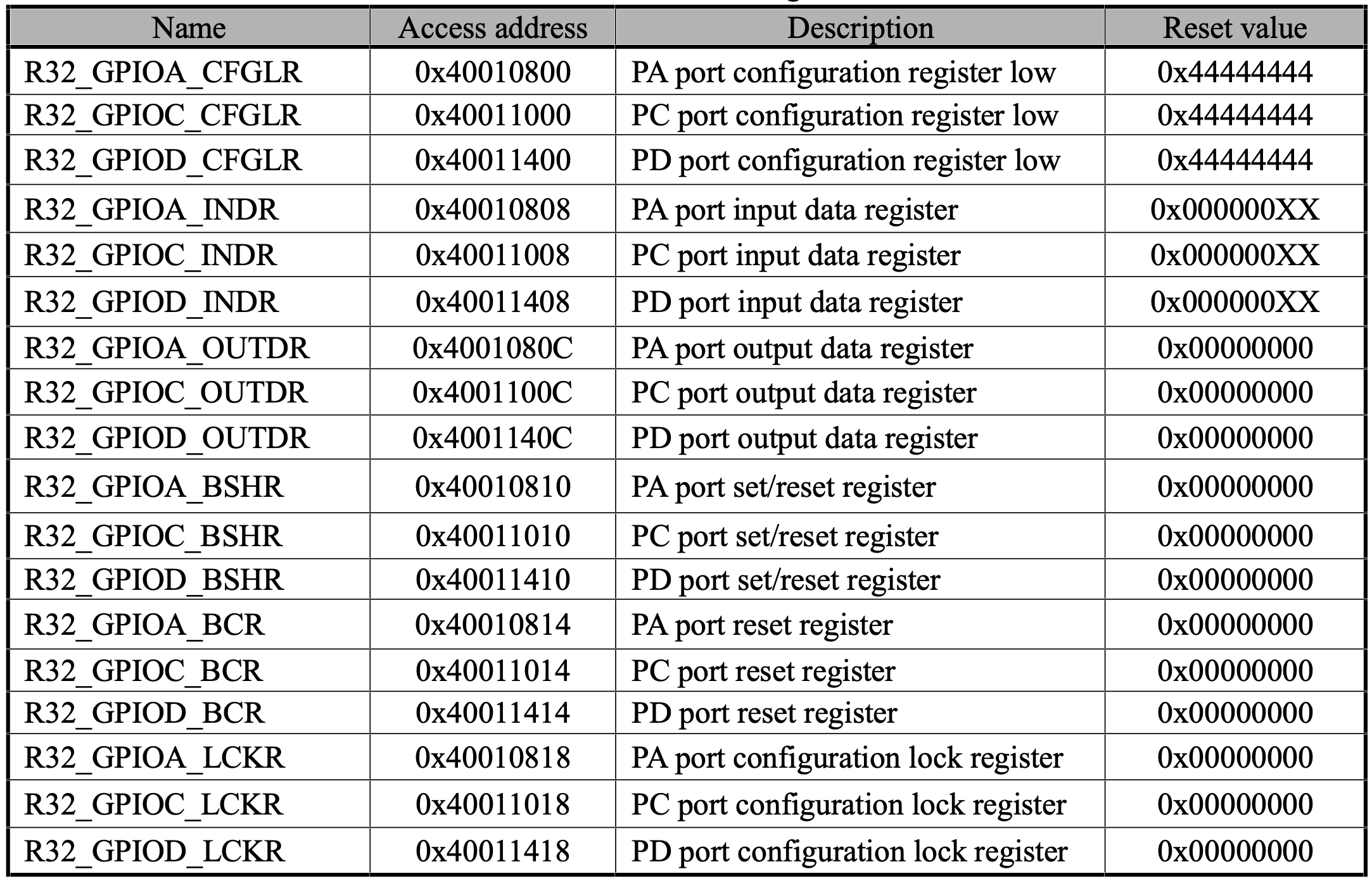
Note: R32_GPIOX_CFGLR address and the next register address, R32_GPIOX_INDR, have an 8 byte difference. Since each register occupies 4 bytes that means there’s a reserved register between them. On other chips of the CH32 family this space is used for R32_GPIOX_CFGHR (Configuration High Register) which controls another 8 pins, doubling the amount of pins for each GPIO port. Even though this register is not present in the CH32V003 it is left blank to maintain register address consistency within the chip family.
More specifically, the R32_GPIOX_CFGLR (Configuration Low Register) is used to configure GPIO port D pins 0-7:
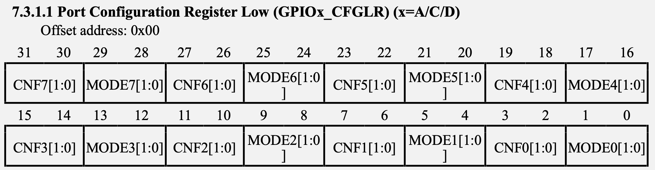
So, if we want to configure pin 4 we have to write to fields MODE4 (bits 16-17) and CNF4 (bits 18-19). To control the LED we want to set MODE4 to 1, which indicates output at 10MHz maximum speed, and CNF4 to 0, which indicates push-pull output mode. Because we don’t want to overwrite the rest of pin configurations we could first perform a bitwise AND with a mask to clear the previous configuration and then bitwise OR the result with the new configuration:
        # clear current pin config with an and mask (shift count determined by pin number * pin conf bit count -> pin*4)
        # GPIOD_CFGLR = GPIOD_CFGLR & ~(0xf << (4*pin)) | ((0|1) << (4*pin))
        lw t0, 0(a2)
        li t1, ~(0x0f << (4 * led_pin))
        and t0, t0, t1

        li t1, 0x00000001 << (4 * led_pin)
        or t0, t0, t1
        sw t0, 0(a2)
System tick counter as timer
The system counter is a device that increments a register value on every clock cycle. It has a special register that allows us to set a comparison value so that when the counter value exceeds the comparison value a flag is set. We can use this to time actions in terms of clock cycles. These are its registers:
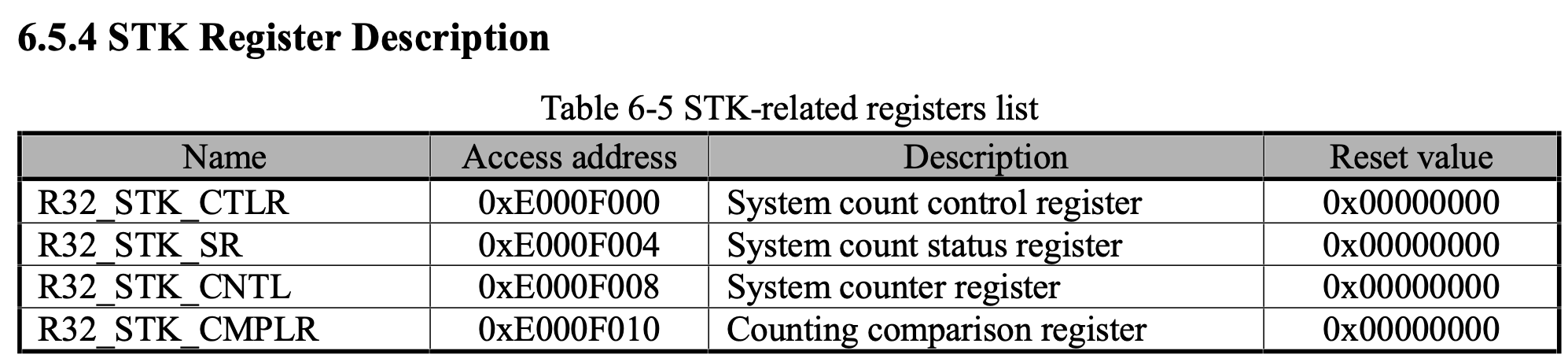
R32_STK_CTLR is used to control the system counter:
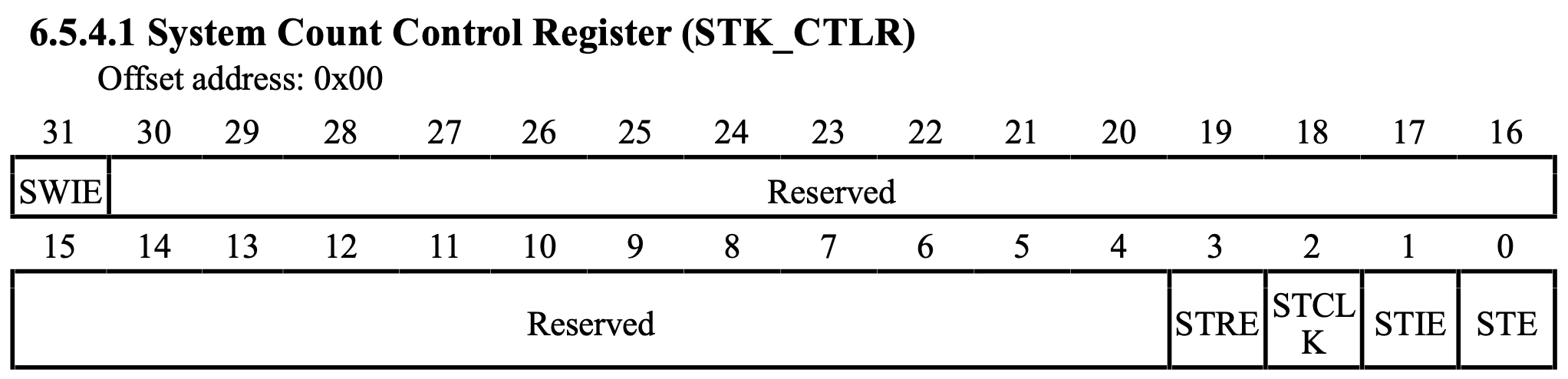
The fields SWIE (software interrupt trigger enable) and STIE (counter interrupt enable) are both used to enable/disabled interrupts. Because we won’t be using interrupts we’ll set them both to 0.
Field STRE (System Tick auto-Reload Enable) is used to configure whether the counter resets to 0 after the comparison values has been reached or if it continues counting up to the maximum value. We don’t really care about this as we’ll stop the counter as soon as we detect the comparison value has been reached.
Field STCLK (system tick clock source) is used to select the counter clock source: HCLK (when set to 1) or HCLK/8 (when set to 0). It doesn’t really matter which setting we use as long as we take it into consideration when calculating the amount of ticks to set the counter to. We’ll use HCLK/8 as clock source as it allows for longer time delays.
Field STE (system tick enable) is used to turn on the counter (when set to 1) or turn it off (when set to 0).
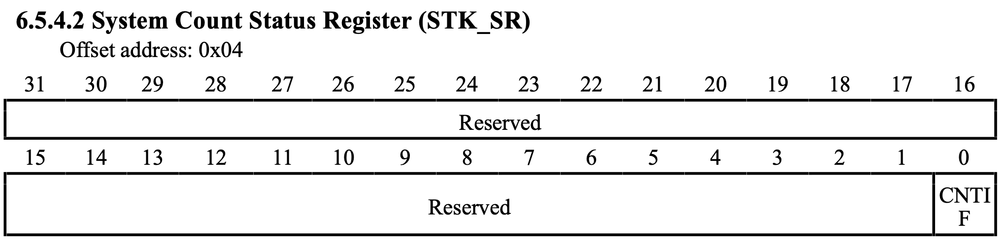
R32_STK_SR has a single 1-bit field, CNTIF, which is set to 1 when the counter reaches the comparison value:
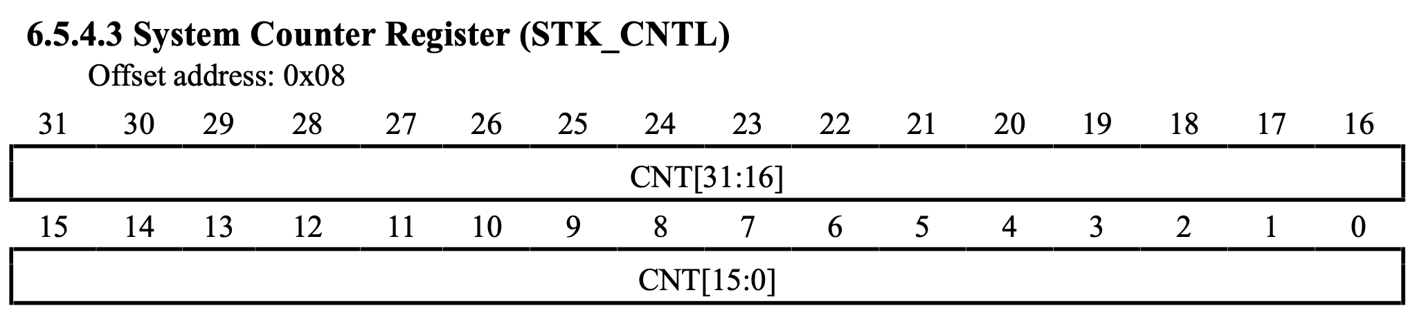
R32_STK_CNTL has a single 32-bit field, CNT, which holds the current counter value:
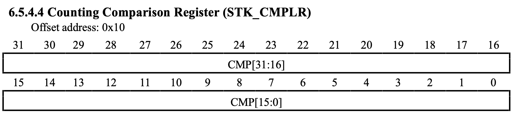
R32_STK_CMPLR has a single 32-bit field, CMP, which holds the comparison value:
Given this set of registers, implementing a system tick delay function is reasonably simple:
- Turn system tick counter off and set clock source as
HCLK/8 - Clear the comparison flag
- Set initial counter value
- Set comparison counter value
- Turn system tick counter on
- Wait until the comparison flag is set
- Turn system tick counter off
Let’s write a function waits until the number of ticks (HCLK/8) in register a0 have been reached:
delay_systick:
        # function prologue
        addi sp, sp, -16
        sw ra, 12(sp)
        sw s0, 8(sp)
        sw s1, 4(sp)

        li s1, systck_base # s1 -> system tick register base address

        # stop system counter (set STE [bit 0] to 0) and select HCLK/8 as clock source (set STCLK [bit 2] to 0)
        # STK_CTLR = STK_CTLR & ~((1<<0) | (1<<2))
        # STK_CTLR = STK_CTLR & ~(0x00000005)
        # STK_CTLR = STK_CTLR & ~(0x00000005)
        # STK_CTLR = STK_CTLR & 0xfffffffa
        lw s0, 0(s1)
        and s0, s0, 0xfffffffa
        sw s0, 0(s1)

        # clear count value comparison flag (set CNTIF [bit 0] to 0)
        # STK_SR = STK_SR & ~(1<<0)
        # STK_SR = STK_SR & 0xfffffffe
        li s0, 0xfffffffe # s0 = ~(1)
        sw s0, 4(s1)

        # set initial counter value
        # STK_CNTL = 0
        sw zero, 8(s1)

        # set count end value
        # STK_CMPLR = a0
        sw a0, 16(s1)

        # start system counter (set STE [bit 0] to 1)
        # STK_CTLR = STK_CTLR | (1<<0)
        # STK_CTLR = STK_CTLR | 0x00000001
        lw s0, 0(s1)
        or s0, s0, 0x00000001
        sw s0, 0(s1)

        # wait until count system counter has reached target number
.L_wait:
        lw s0, 4(s1) # s0 = STK_SR
        and s0, s0, 0x00000001 # s0 = STK_SR & 0x00000001
        beq s0, zero, .L_wait # if s0 != 0 -> bit 0 is set -> count has been reached

        # stop system counter (set STE [bit 0] to 0)
        # STK_CTLR = STK_CTLR & ~(1<<0)
        # STK_CTLR = STK_CTLR & 0xfffffffe
        lw s0, 0(s1)
        and s0, s0, 0xfffffffe
        sw s0, 0(s1)

        # function epilogue
        lw s1, 4(sp)
        lw s0, 8(sp)
        lw ra, 12(sp)
        addi sp, sp, 16

        ret
Making the LED blink
Now all that remains is to actually make the LED blink by setting GPIO D4 high and low in between delay_systick calls. There are two registers we can use to set any given GPIO pin high or low.
R32_GPIOX_BCR is only used to reset (set to low state) any pin in the GPIO port by writing a 1 to the corresponding field:
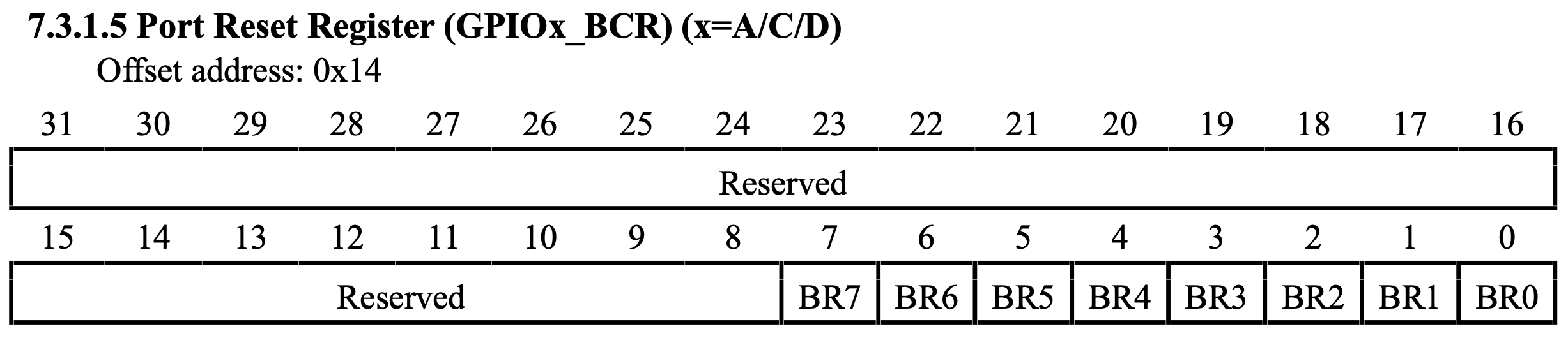
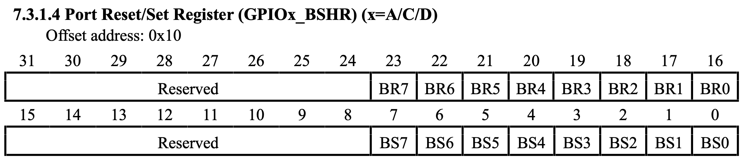
R32_GPIOX_BSHR is used for both setting (set to high state) and resetting (set to low state) any given pin in the GPIO port. Works identically to R32_GPIOX_BCR but the set fields are on the lower 16 bits and the reset fields are on the higher 16 bits. This register is useful for setting and resetting different pins at the same time and in scenarios where immediate execution of the next instruction is not guaranteed (when interrupts are enabled or on multicore CPUs) because it can be done in a single atomic operation.
Because we want to have the LED on and off for a certain amount of time we have to convert that amount to number of system ticks in order to use the delay_systick function. For a 48MHz system clock source we could calculate the milisecond to tick factor the following way:
$$ \frac{48000000cycle}{1s} \cdot \frac{1tick}{8cycle} \cdot \frac{1s}{1000ms} = 6000 ticks/ms $$
Finally, we can write an infinite loop to blink the LED:
        li t2, 1 << led_pin # pin mask
.L_loop:
        sw t2, 20(a2) # GPIO_BCR = (1 << led_pin)
        li a0, 100*ms_to_tick # keep led on for 100ms
        call delay_systick

        sw t2, 16(a2) # GPIO_BSHR = (1 << led_pin)
        li a0, 1000*ms_to_tick # keep led off for 1000ms
        call delay_systick

        j .L_loop
And if we put it all together:
.section .text

.equ ms_to_tick, 48000000/8000

.equ rcc_base, 0x40021000
.equ flash_r_base, 0x40022000
.equ gpio_pd_base, 0x40011400
.equ systck_base, 0xe000f000

.equ led_pin, 4

.globl main
main:
        # setup clock to 48MHz
        li a0, rcc_base # a0 -> RCC register base address
        li a1, flash_r_base # a1 -> FLASH register base address
        li a2, gpio_pd_base # a2 -> GPIO port d register base address

        # PLL_ON (bit 0): enable PLL
        # HSI_ON (bit 24): enable HSI
        #     RCC_CTLR = 1 << 0 | 1 << 24
        #     RCC_CTLR = 0x01000001
        li t0, 0x01000001
        sw t0, 0(a0)

        # HPRE = 0: prescaler off; do not divide SYSCLK
        # PLLSRC = 0: HSI (instead of HSE) for PLL input
        #     RCC_CFGR0 = 0 << 4 | 0 << 16
        #     RCC_CFGR0 = 0
        li t0, 0x00000000
        sw t0, 4(a0)

        # configure flash to recommended settings for 48MHz clock
        # LATENCY (bits 0-1) = 1
        #     FLASH_ACTLR = 1 << 0
        #     FLASH_ACTLR = 1
        li t0, 0x00000001
        sw t0, 0(a1)

        # CSSC     (bit 23) = 1 -> clear CSSF (clock security system interrupt flag bit)
        # PLLRDYC  (bit 20) = 1 -> clear PLLRDYF (PLL-ready interrupt flag bit)
        # HSERDYC  (bit 19) = 1 -> clear HSERDYF (HSE oscillator ready interrupt flag bit)
        # HSIRDYC  (bit 18) = 1 -> clear HSIRDYF (HSI oscillator ready interrupt flag bit)
        # LSIRDYC  (bit 16) = 1 -> clear LSIRDYF (LSI oscillator ready interrupt flag bit)
        # PLLRDYIE (bit 12) = 0 -> disable PLL-ready interrupt
        # HSERDYIE (bit 11) = 0 -> disable HSE-ready interrupt
        # HSIRDYIE (bit 10) = 0 -> disable HSI-ready interrupt
        # LSIRDYIE (bit  8) = 0 -> disable LSI-ready interrupt
        #     RCC_INTR = 1<<23 | 1<<20 | 1<<19 | 1<<18 | 1<<16 | 0<<12 | 0<<11 | 0<<10 | 0<<8
        #     RCC_INTR = 0b 0000 0000 1001 1101 0000 0000 0000 0000
        #     RCC_INTR = 0x009d0000
        li t0, 0x009d0000
        sw t0, 8(a0)

        # wait until PLL is ready
        li t1, 0x02000000 # PLL_RDY mask
.L_pll_rdy_wait:
        lw t0, 0(a0) # RCC CTLR
        and t0, t0, t1
        beq t0, zero, .L_pll_rdy_wait

        # RCC_CFGR0 = RCC_CFGR0 & ~(0b11) | 0b10
        # RCC_CFGR0 = RCC_CFGR0 & ~(0x00000003) | 0x00000002
        # RCC_CFGR0 = RCC_CFGR0 & 0xfffffffc | 0x00000002
        lw t0, 4(a0) # t0 = RCC CFGR0
        and t0, t0, 0xfffffffc # ~(RCC CFGR0 SW) = ~(0x00000003) = 0xfffffffc
        or t0, t0, 0x00000002 # RCC CFGR0 SW PLL = 0x00000002
        sw t0, 4(a0)

        # wait until PLL is used as SYSCLK
        li t1, 0x0000000c # RCC CFGR0 SWS mask
        li t2, 0x00000008 # RCC CFGR0 SW PLL
.L_pll_use_wait:
        # RCC CFGR0
        lw t0, 4(a0)
        and t0, t0, t1
        bne t0, t2, .L_pll_use_wait

        # setup GPIO pin for led
        # enable GPIO port D
        lw t0, 24(a0) # t0 = APB2PCENR
        or t0, t0, 0x00000020 # APB2PCENR | EPB2PCENR_IOPDEN
        sw t0, 24(a0)

        # clear current pin config with an and mask (shift count determined by pin number * pin conf bit count -> pin*4)
        # GPIOD_CFGLR = GPIOD_CFGLR & ~(0xf << (4*pin))
        lw t0, 0(a2)
        li t1, ~(0x0f << (4 * led_pin))
        and t0, t0, t1

        # set new pin config with an or
        # GPIOD_CFGLR = GPIOD_CFGLR | ((0|1) << (4*pin))
        li t1, 0x00000001 << (4 * led_pin)
        or t0, t0, t1
        sw t0, 0(a2)

        li t2, 1 << led_pin # pin mask
.L_loop:
        sw t2, 20(a2)
        li a0, 100*ms_to_tick
        call delay_systick

        sw t2, 16(a2)
        li a0, 1000*ms_to_tick
        call delay_systick

        j .L_loop

delay_systick:
        # function prologue
        addi sp, sp, -16
        sw ra, 12(sp)
        sw s0, 8(sp)
        sw s1, 4(sp)

        li s1, systck_base # s1 -> system tick register base address

        # stop system counter (set STE [bit 0] to 0) and set HCLK/8 as clock source (set STCLK [bit 2] to 0)
        # STK_CTLR = STK_CTLR & ~((1<<0) | (1<<2))
        # STK_CTLR = STK_CTLR & ~(0x00000005)
        # STK_CTLR = STK_CTLR & ~(0x00000005)
        # STK_CTLR = STK_CTLR & 0xfffffffa
        lw s0, 0(s1)
        and s0, s0, 0xfffffffa
        sw s0, 0(s1)

        # clear count value comparison flag (set CNTIF [bit 0] to 0)
        # STK_SR = STK_SR & ~(1<<0)
        # STK_SR = STK_SR & 0xfffffffe
        li s0, 0xfffffffe # s0 = ~(1)
        sw s0, 4(s1)

        # set initial counter value
        # STK_CNTL = 0
        sw zero, 8(s1)

        # set count end value
        # STK_CMPLR = a0
        sw a0, 16(s1)

        # start system counter (set STE [bit 0] to 1)
        # STK_CTLR = STK_CTLR | (1<<0)
        # STK_CTLR = STK_CTLR | 0x00000001
        lw s0, 0(s1)
        or s0, s0, 0x00000001
        sw s0, 0(s1)

        # wait until count system counter has reached target number
.L_wait:
        lw s0, 4(s1) # s0 = STK_SR
        and s0, s0, 0x00000001 # s0 = STK_SR & 0x00000001
        beq s0, zero, .L_wait # if s0 != 0 -> bit 0 is set -> count has been reached

        # stop system counter (set STE [bit 0] to 0)
        # STK_CTLR = STK_CTLR & ~(1<<0)
        # STK_CTLR = STK_CTLR & 0xfffffffe
        lw s0, 0(s1)
        and s0, s0, 0xfffffffe
        sw s0, 0(s1)

        # function epilogue
        lw s1, 4(sp)
        lw s0, 8(sp)
        lw ra, 12(sp)
        addi sp, sp, 16

        ret
Startup code & linker script
I don’t want to go too much into detail in this section as it isn’t really the purpose of this post and I risk making incorrect statements as this is my first RISC-V low level “deep dive”. Nevertheless, I will go through some aspects I consider important.
This section has been taken almost entirely from the manufacturer’s PlatformIO example startup code. I only have simplified and/or expanded upon it.
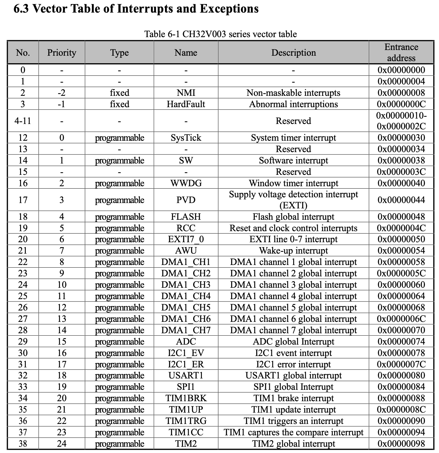
Before the microcontroller can jump to the main symbol and execute our code we should setup some stuff. Most notably, because this microcontroller supports interrupts, we should setup the interrupt vector table so that if an interrupt/exception were to happen it is handled correctly without any unexpected behaviour. To do this, we have four CSR registers:
The first two are RISC-V standard CSRs and do not appear in the manual (here’s a blog I found that documents their layout: MSTATUS, MEPC):
MSTATUS (Machine Status Register) with address 0x300 which controls the processor’s global state, particularly privilege levels and interrupt enables. For our use case, field at bit 3 MIE (Machine Interrupt Enable) which enables interrupts when set to 1 and field at bit 7 MPIE (Machine Previous Interrupt Enable) which holds the previous interrupt enable state (before entering an interrupt/exception handler) and is used to restore the value of MIE when returning from an interrupt handler (with the mret instruction).
MEPC (Machine Exception Program Counter) with address 0x341 which holds the program counter when an exception or interrupt occurs so that the exception handler can properly return.
The last two are actually vendor-specific and are listed on the manual. The first one, although it is a RISC-V standard, has been extended to allow for more configuration options:
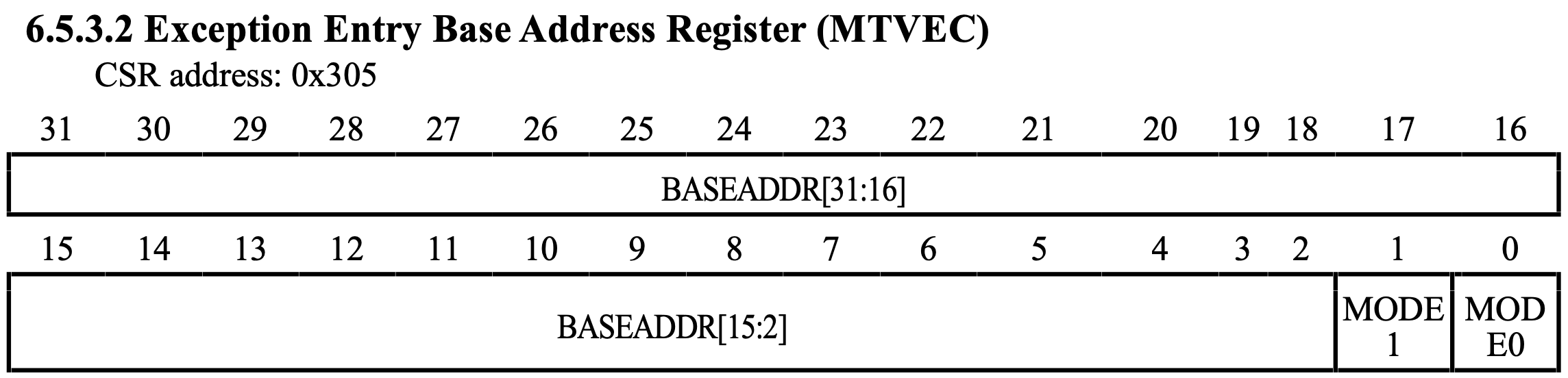
Field BASEADDR (bits 2-31) indicates the base address for the interrupt vector. Initially, it points to address 0x00000000 which is the entry address (the first instruction the microcontroller executes upon reset). Also, notice how the last two bits are not part of this field despite the address space being 32-bit. This is because the interrupt vector address must be 4-byte aligned and the two least significant bits are hardwired to 0.
Field MODE1 (bit 1) selects the interrupt table identification pattern: when set to 1 the microcontroller expects every entry of the interrupt vector to be a jump instruction to the handler, when configured to 0 it expects the absolute address of the handler.
Field MODE0 (bit 0) selects the interrupt entry address mode: when set to 0 all interrupt handlers will have the same handler entry address, when set to 1 each interrupt handler will be offset by the interrupt_number * 4 so the address of the handler for interrupt number n will be BASEADDR + n*4 with the following layout:
The second one, INTSYSCR is a completely custom CSR:
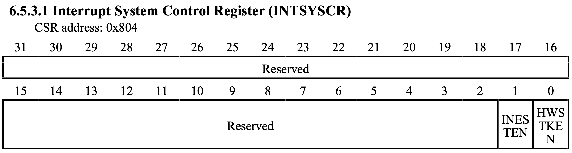
Field INESTEN (bit 1) enables interrupt nesting when set to 1, and disables it when set to 0.
Field HWSTKEN (bit 0) enables hardware stacking when set to 1, and disables it when set to 0.
So there are a few configuration options to choose from and because in our case it doesn’t really matter what we choose I have chosen the following configuration:
- interrupt nesting and hardware stacking enabled
- interrupt vector with offsets instead of a unified entry address
- interrupt vector with absolute addresses instead of jump instructions
- all interrupt handlers point to function which loops forever
With this in mind we could write the following entry function, start, which also acts as the reset handler:
.section .init
.globl start
start:
        # there isn't really a need for setting up gp since it isn't used in this program
.option push
.option norelax
        la gp, __global_pointer$
.option pop
        la sp, __stack_end

        # set CSR register MSTATUS (Machine Status)
        #     bit 7: MPIE (Machine Previous Interrupt Enable) to 1, which will enable interrupts when mret is executed
        #     bit 3: MIE (Machine Interrupt Enable) to 0, which disables interrupts
        li t0, 0x80
        csrw mstatus, t0

        # set CSR register INTSYSCR (Interrupt System Control Register) located at CSR address 0x804
        #     bit 1: interrupt nesting table enable to 1
        #     bit 0: hardware stack enable to 1
        li t0, 0x3
        csrw 0x804, t0

        # set CSR register MTVEC (Exception Entry Base Address Register)
        #     bits [31:2]: interrupt vector table base address (aligned to 4 bytes; last two bits are hardwired to 0)
        #     bit 1: indentify pattern -> 1 : by absolute address
        #     bit 0: entry address -> 1 : address offset based on interrupt number*4
        la t0, isr_vector
        ori t0, t0, 3
        csrw mtvec, t0

        # set CSR register MEPC (Machine Exception Program Counter); return address of an exception handler
        la t0, main
        csrw mepc, t0
        mret
        # mret -> Machine Return (return from exception handler)
        #     1. restore MIE from MPIE
        #     2. set MPIE to 1
        #     3. jump to address stored in MEPC CSR register

.section .text.isr_handler

.align 2
isr_default:
        j isr_default

.align 2
.option norvc
isr_vector:
        .word  start
        .word  0
        .word  isr_default
        .word  isr_default
        .word  0
        .word  0
        .word  0
        .word  0
        .word  0
        .word  0
        .word  0
        .word  0
        .word  isr_default
        .word  0
        .word  isr_default
        .word  0
        .word  isr_default
        .word  isr_default
        .word  isr_default
        .word  isr_default
        .word  isr_default
        .word  isr_default
        .word  isr_default
        .word  isr_default
        .word  isr_default
        .word  isr_default
        .word  isr_default
        .word  isr_default
        .word  isr_default
        .word  isr_default
        .word  isr_default
        .word  isr_default
        .word  isr_default
        .word  isr_default
        .word  isr_default
        .word  isr_default
        .word  isr_default
        .word  isr_default
        .word  isr_default
Note: the gp (global pointer) initialization is a RISC-V standard but it isn’t really needed here.
Now we have the completed code but, even though the we can compile the assembly code, we can’t upload the raw object file because the microcontroller will not know how to interpret it. We have to create a linker script to specify the linker how to structure the resulting binary. Here’s a simplified version of the linker script found at the manufacturer’s PlatformIO repository:
ENTRY(start);

PROVIDE(__stack_size = 256);

MEMORY {
	FLASH (rx) : ORIGIN = 0x00000000, LENGTH = 16K
	RAM (rwx)  : ORIGIN = 0x20000000, LENGTH = 2K
}

SECTIONS {
	.init : {
		. = ALIGN(4);
		PROVIDE(__start = .);
		KEEP(*(SORT_NONE(.init)));
		. = ALIGN(4);
	} >FLASH AT>FLASH

	.text : {
		. = ALIGN(4);
		*(.text);
		*(.text.*);
		*(.rodata);
		*(.rodata.*);
		. = ALIGN(4);
	} >FLASH AT>FLASH

	.data : {
		. = ALIGN(4);
		*(.data .data.*)
		PROVIDE(__data_start = .);
		. = ALIGN(8);
		/* since gp is used to access globals within +/-2KB and total RAM size is 2KB
		 * we can just set it to the base of the .data section */
		PROVIDE(__global_pointer$ = .);
		. = ALIGN(8);
		PROVIDE(__data_end = .);
	} >RAM AT>FLASH

	.stack ORIGIN(RAM) + LENGTH(RAM) - __stack_size : {
		PROVIDE(__heap_end = .);
		. = ALIGN(8);
		PROVIDE(__stack_start = .);
		. = . + __stack_size;
		PROVIDE(__stack_end = .);
	} >RAM
}